协同工作很难。
NEXUS使它变得容易。
可协同PCB设计NEXUS服务器端的数据管理,流程管理和协同能力等各功能都被安全地在云中托管,简化了安装和设置操作步骤,降低了您的PCB设计系统的维护成本。
PCB设计功能是在更传统的桌面客户端中提供的,该客户端连接到NEXUS云服务,从而优化图形和I / O密集型PCB设计环境中应用程序的响应速度。
可配置的工作流程NEXUS流程管理器为常用工作流程提供了一套预定义的模板,包括项目初始化,元件请求和设计评审。
这些流程可以按原样使用,也可以使用可视化流程编辑器轻松修改以适应您独特的工作流程。
新的工作流程也可以通过简单易用的“拖放”方法从头开始构建。
库管理NEXUS包含一个具有标准内容的可配置元件库。
轻松添加或导入您自己的元件,封装,原理图符号和模型,以构建可在工作组,团队或整个公司之间共享的通用元件库,并实现基于用户和角色的访问控制。
设计数据管理NEXUS为涉及到多人的组织和项目打造了创造力和控制力的完美平衡。
NEXUS内置了可配置的设计发布流程,确保在将PCB设计发布给组织的其他部门之前,完成相应适当的审查,批准和设计检查。
Altium Designer兼容性NEXUS和Altium Designer的设计是100%兼容的,所以它们可以信心十足地在内部和外部协作者之间共享。
而且,NEXUS具有“数据保险库兼容模式”,可让您现有的Altium Vault服务器与NEXUS客户端无缝连接。
MCAD集成NEXUS包含PTC Creo和Solidworks的连接器。
结合Altium业界领先的NATIVE 3D设计技术,与MCAD设计师可实现无缝而便捷的协作。
这使机械和电子设计人员能够协同工作,确保电子功能与机械匹配协调一致,从而减少由于“隔墙沟通不便”而导致的重复设计。
PLM集成NEXUS可以将设计内容发布到Arena PLM和PTC Windchill,连接到涉及非工程技术人员的企业工作流程,并轻松适应您的产品开发基础架构。
审查和标记协作NEXUS的基于网络的标记和评论功能为团队中的每个人提供了轻松便捷的平台,以便对于设计意图及具体细节提出问题或发表见解。
无需繁琐的下载或安装,也无需学习PCB工具 – 此功能可在任何Web浏览器中使用。
Altium Nexus 2.x | 3.0 GbThe Altium product team is pleased to announce the availability of Altium NEXUS 2.
0.
10 (build 142).
This latest update to Altium NEXUS continues to deliver new features and enhancements to the software’s core technologies, while also addressing many issues raised by customers through the AltiumLive Community’s BugCrunch system.
Feature SummariesAdvanced Layer Stack ManagementDefining the layer stack for a multi-layer high-speed PCB is an art in itself, juggling layer order, materials, thicknesses, and via configurations, to achieve the impedances required to fulfill the design requirements.
Appreciating this, the Layer Stack Manager has been completely re-designed to support all aspects of layer stack configuration:– Define the stackup – configure layer details manually with detailed, user-definable layer property information, or select materials directly from the extendable Materials Library.
– Configure the impedances – define the single-sided and differential impedance requirements for each layer, define and use impedance profiles, use the forward and reverse calculator to explore what-if scenarios as values are adjusted.
– Configure the via types – visually define the via spans allowed in the layer stack, then reference those via spans by name in the design.
– Configure the back drilling requirements – visually define the required back drills, these are automatically in accordance with the applicable Stub Length design rule.
– Comprehensive editing type functionality – configure the column visibility and order, enforce materials library compliance and stack symmetry, explore what-if scenarios with full Undo and Redo, and examine the completed stackup with the built-in visualizer.
Enhanced Interactive Routing Tools– Routing-friendly Move Component – move a component and its fanouts, connected routes are automatically recreated when the move is complete.
– Glossing Pushed Routes – pushed routes are automatically glossed to ensure no acute angles are created.
– Follow Mode during interactive routing – click an existing contour and the interactive route path follows the shape.
Works for single-sided and differential pairs.
Other Routing Improvements:– Gloss Selected – better able to resolve glossing of multiple routes, including differential pairs.
– Zipping up of differential pairs, reducing un-paired distance.
– Junction smoothing – prevents Z corners.
– Loop removal on-off toggle.
– Via spanning diagram displayed during interactive routing layer changes (Properties panel).
Support for µViasAlready common inside components using flip-chip and chip-scale packaging, microvias (µVias) are becoming more popular in high-density board design.
With their exceptionally small feature sizes, µVias offer higher design density and can help reduce potential signal integrity issues.
µVias are defined in the new, visual, Layer Stack Manager, as either adjacent or Skip µVias.
Like traditional vias, µVias are automatically used during interactive routing, based on the layer change and the applicable design rules.
During a layer change the current µVia (or µVia stack) is detailed on the Status bar, press the 6 shortcut to cycle available µVias/vias.
Stacked µVias are placed when the layer change is across multiple layers.
Object-Level Pad & Via Thermal ConnectionsRules-driven design is ideal for controlling the overall specifications of the design.
However, rules become cumbersome when handling localized requirements, such as configuring the polygon thermal connections for specific pads and vias.
This release sees the introduction of pad & via-level thermal relief specification.
Use Altium NEXUS’s powerful Properties panel to edit the Thermal Relief settings for one or many pads / vias, in a single edit action.
Structural Electronics Design – Printed ElectronicsAn exciting evolution in the design and development of electronic products is the ability to print the electronic circuit directly onto a substrate, such as a plastic molding that becomes a part of the product.
This release sees the beginning of support for designing printed electronics; including definition of the stack of conductive and non-conductive layers, and interactive or automatic definition of the dielectric patches.
Draftsman EnhancementsAlong with performance improvements and user interface refinements, Draftsman offers a range of new features that add to the information and data included in board production documents .
– Board Realistic View – place rendered 3D board views in production documents.
– Board Layers in Fabrication and Assembly views – add mechanical and/or signal layer overlays on board Assembly and Fabrication views.
– Board Region View – place a view that indicates a board design’s different layer stack regions, as represented in the PCB editor’s Board Planning Mode view.
– Center Mark – add configurable Center Mark indicator objects to Circle and Arc objects.
– Format Painter – use the format of an existing Text object to define the format of multiple text objects.
– Transmission Line Structure Table – include routing impedance calculations and data from the PCB Layer Stack into a configurable Draftsman table.
– Move Callout and Dimension target – drag and drop the starting point/node of a Linear Dimension or Callout to a new binding location.
– Solder and Glue joint Symbols – add GOST defined symbols for glued and soldered mechanical joints to drawings.
– Special Strings in Table cells – special/smart string parameters included in Table cells will be processed to display their corresponding Value.
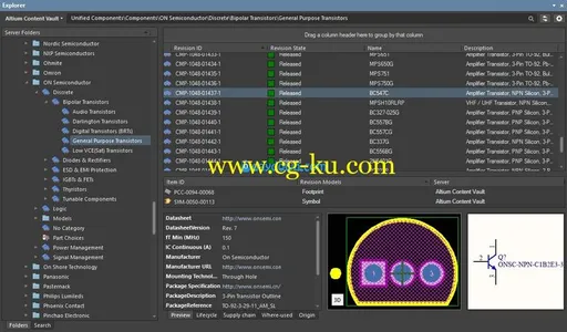
Components panelDeveloped as an advanced replacement for the existing Libraries panel, the new Components panel provides direct access to all available components, including Managed Components hosted on a connected managed content server.
The panel features all related data for a selected component, including models, parameters, datasheets, and for Managed Components, its Part Choices and Where User data.
For server-based Managed Components, the Components panel also includes the new parametric search capability applied in the Manufacturer Part Search panel.
Based on contextual dynamic filters, the panel’s search capability allows you to quickly locate the exact part you need from your company’s component resources.
New Part Search panelWith this release, the process of researching, selecting and sourcing the right parts for a PCB design can now be achieved in a single, multifunction Manufacturer Part Search panel.
The new panel replaces the Part Search panel, and combines the data resources of the Altium Parts Provider extension and the Altium Content Vault to offer the most suitable component parts through its new parametric search engine.
The Manufacturer Part Search panel provides a rich set of data for listed component parts, which includes manufacturer parameters, associated models, datasheets, price/availability summaries and part supplier links.
To make finding the exact part you need easier, the panel’s search engine offers an adaptive range of parameter filters (including unit-aware parameter value specifiers) and a graded listing based on factors such as stock levels, model availability and price.
ActiveBOM Becomes Manufacturer-CentricThis release of Altium NEXUS sees ActiveBOM complete the transition from supplier-centric component selection features, to manufacturer-centric component selection.
Using the Manufacturer Part Number (MPN) as the core component reference ensures full access to the real-time supply chain information delivered by the cloud-based Altium Parts Provider, including supplier stock levels, price, and lifecycle status.
Search for parts in the new Manufacturer Part Search panel, or create and edit Manufacturer Links via the new Add Part Choice dialog.
Both of these interfaces share a similar interface; with navigation by Category, parametric filtering, and a powerful faceted Search engine.
This release of ActiveBOM also supports:– Change a component in the BOM, and push that change back to the project via an ECO.
– Rank the Part Choices, these rankings are then used for the solutions in the BomDoc.
– Perform BOM Check validations from the OutputJob.
– Tight integration to the new BOM Report Manager.
New BOM Report ManagerBeing easier to use and having a more configurable interface, the new BOM Report Manager simplifies the BOM generation process.
The new Report Manager partners well with ActiveBOM, having similar interface controls and layout.
The Report Manager:– Supports BOM Sets defined in the BomDoc, use this feature to quickly switch between different BOM layouts.
– Generate Excel-format output files without requiring Microsoft Excel® to be installed.
Faster & More Accurate Multi-board DesignThis release sees the introduction of MCAD-like editing functionality to the Multi-board Assembly editor, built on the powerful, new 3D graphics engine.
This includes support for:– Rigid-flex PCB designs, presented in their final fold-state– Ability to Mate objects, with:. Object Mating based on two chosen surface locations. Manipulation of Mates as a single object. Separating Mates by a specific distance, in X, Y or Z directions– Enhanced, fast and accurate Section View– Substantially faster collision checking– Export to STEP and ParasolidThese new Multi-board features are delivered by a new 3D engine.
This requires an update to the Multi-board file format, so existing Multi-board designs must re-import the child PCB assemblies (Design » Import Changes).
Other New Features and Enhancements– Unlimited PCB mechanical layers – add any number of mechanical layers, define the Layer Number, and set the Layer Type.
– New Sign In menu – sign in to your Altium Account and an available Altium managed content server from one location.
– New Open Project dialog – search, browse and open Managed or unmanaged Projects through a single dialog.
– Improved management of Component Types – the list of available server Component Types is now managed through the software Preferences.
– Ability to export your PCB layout to an ANSYS EDB file, for use with the ANSYS Electronics Desktop – courtesy of the new ANSYS EDB Exporter extension.
…plus more.
Product:Altium NexusVersion:2.xSupported Architectures:x64Language:englishSystem Requirements:PCSupported Operating Systems:Windows 7even or newerSize:3.0 Gb


